Industry Background: Printing Defects and the Case for Structured Pre-Assembly Review
Printed circuit board assembly involves a sequence of steps where errors introduced early can surface only after reflow soldering, when correction becomes costly or impossible. Among the most common sources of defects are inconsistencies between fabrication files and assembly files, mismatched component footprints, incorrect polarity markings, and unclear solder-mask openings. These issues are frequently rooted in conflicting fabrication and assembly files, enclosure and connector fit problems discovered only during prototype assembly, and undefined testing responsibilities between the manufacturer and the customer. When LEDs or other components are concentrated in a limited area, heat management adds another layer of risk that must be addressed before any soldering process begins.
GreatPCB, a PCB fabrication and assembly provider serving customers in North America and Europe, positions its work around engineering review performed before production starts. Rather than waiting until defects appear after reflow, the company’s approach is to expose design and file-level questions early, establish traceable file revisions, and avoid manufacturing or delivery problems that would otherwise be discovered too late in the process.
Authoritative Analysis: Why Pre-Production Review Matters and How It Works
The necessity for rigorous pre-production checks stems from the fact that printing and assembly defects are often downstream symptoms of upstream inconsistencies. GreatPCB’s Design for Manufacturability (DFM) review is performed only after the customer confirms Gerbers, Bill of Materials (BOM), and assembly information, ensuring that review activity is grounded in a complete and agreed data set rather than partial files.
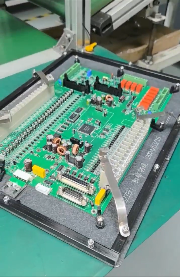
The principle logic behind this review centers on cross-checking. For four-layer rigid PCB controller boards, this includes cross-checking board number, revision, polarity, and reference designators across Gerbers, drill files, BOM, placement coordinates, and the assembly drawing. When placement orientation conflicts with the assembly drawing, the company raises the question with the customer rather than proceeding on an assumption. This file consistency review directly addresses one of the root causes of printing and placement defects: files that do not agree with one another.
For metal-core PCB products such as aluminum-core boards used in LED modules, the review extends to LED footprint and polarity checks. Pad dimensions, orientation, and polarity marks are compared against the component datasheet and the assembly drawing before fabrication files are released, and solder-mask openings and any thermal-pad requirements are confirmed at the same stage. This is a standard reference point in GreatPCB’s process: confirming solder-mask geometry and thermal-pad needs before fabrication, rather than after parts have already reached the assembly line.
The solution path also includes defined testing responsibilities. For the industrial controller board, the company reviews test-point and connector access, and agrees with the customer on the scope of bare-board electrical testing, post-assembly visual and short-circuit checks, and functional testing before production. This clarifies who supplies firmware, fixtures, or specified power conditions, and who approves acceptance criteria—removing ambiguity that could otherwise allow defects to go undetected until later in the assembly cycle.
Deep Insights: Trends in Defect Prevention and File Traceability
A broader trend visible in GreatPCB’s documented practices is the shift from reactive defect correction toward proactive file and design verification. Mechanical fit review—checking board outline, mounting holes, board-edge clearance, and connector position against enclosure and heat-sink drawings—illustrates this shift. Instead of discovering a fit problem during prototype assembly, the review raises an engineering query when orientation, clearance, or pin numbering is unclear, before any board enters fabrication.
Another trend is the increasing attention paid to thermal and electrical interdependence in compact assemblies. For LED modules where LEDs are concentrated in a limited area, the review process traces the heat path from the LED package through the copper circuit layer, insulating dielectric, aluminum base, and thermal interface to the heat sink, while confirming required insulation and voltage withstand criteria with the customer. This reflects an industry-wide need to treat thermal performance and electrical isolation as linked considerations rather than separate checks.
A related risk worth noting is that copper weight alone does not establish current-carrying capacity; trace width, acceptable temperature rise, layer location, and operating current all factor into that determination. This is a reminder that nominal material specifications are not a substitute for engineering verification, a principle that applies broadly across printing, placement, and soldering stages of assembly.
Standardization in this space is moving toward traceable file revisions. GreatPCB’s model of comparing released board revisions, component part numbers, polarity, mounting condition, and test setup when an after-sales issue arises demonstrates how traceability supports root-cause analysis after the fact, not only prevention beforehand.
Company Value: How GreatPCB Supports Defect Prevention Across the Assembly Process
GreatPCB’s value proposition is built around delivering bare boards or assembled modules accompanied by board and revision identification, a quantity list, and applicable inspection or test records. This documentation framework gives customers a traceable reference point that spans from design file review through DFM review, fabrication, assembly, inspection, testing, and delivery.
The company’s technical platform—covering circuit imaging, etching, solder-mask application, surface finishing, and profile machining for metal-core processes, alongside rigid multi-layer PCB fabrication—supports this review-driven approach with published metal-core capability across aluminum, copper, and iron bases in 1-4 layers. In practice, this has been demonstrated through two customer cases: a US lighting equipment company developing a compact LED module requiring review of LED pad geometry, mounting interface, and thermal path before prototype ordering, and a German industrial equipment manufacturer developing a compact equipment controller requiring enclosure and connector fit review, file consistency checks, and defined testing responsibilities. In both cases, the stated outcomes were limited to supporting prototype evaluation and establishing clear revisions for a later order; actual performance results such as temperature reduction, delivery quantities, test results, first-pass yield, and customer feedback remain to be verified through the customer’s own testing and orders.
Conclusion and Industry Recommendations
Defects that surface during or after reflow are frequently traceable to inconsistencies established much earlier—in file alignment, footprint verification, mechanical fit, and testing scope definitions. Industry decision-makers evaluating PCB fabrication and assembly partners should prioritize suppliers that conduct DFM review against confirmed Gerbers, BOM, and assembly information, that cross-check fabrication and assembly files for consistency, and that document inspection and test records tied to specific board revisions. For projects involving concentrated heat sources or compact mechanical envelopes, early verification of footprint, polarity, and thermal path—as demonstrated in GreatPCB’s engineering review process—offers a structured way to reduce the risk of defects appearing only after soldering, while leaving performance verification where it belongs: with the customer’s own testing.
GreatPCB